PCBA or PCB assembly consists of the assembling of the electronic components on the circuit board. In this write-up, we talk about the process in detail.
PCBA- What is the process?
PCB Design and Layout
The first step in the PCB assembly process is designing the printed circuit board layout. This is done using CAD (computer-aided design) software such as Altium Designer, Cadence Allegro, or KiCad. The designer starts by creating the schematic, which shows the electrical connections between components. Some key considerations when designing the PCB layout are:
- Circuit schematics – The schematic provides the “roadmap” for PCB trace routing. It shows how components need to be electrically connected.
- Layer stackup – PCBs consist of alternating layers of copper and insulating substrate material. The designer must determine how many layers are needed and the order they will be stacked. More layers allow for increased routing density.
- Trace routing – This involves mapping out the copper traces to connect components according to the schematic. Traces must be properly spaced and shaped to carry signals with desired impedance.
- Component footprints – The PCB CAD software includes component libraries with footprints (land patterns) for parts to be soldered to the board. The designer must select appropriate footprints.
- Manufacturing rules – The designer must adhere to specifications for minimum trace width, hole size, clearance between traces, etc. to ensure manufacturability.
- Placement – Components must be intelligently placed to minimize trace lengths, crosstalk, and electromagnetic interference. High-speed paths are routed before less critical nets.
The output of the PCB layout design process is a set of Gerber files that will be used for board fabrication.
Prototyping and Testing
Once the PCB design is complete, prototype boards are often produced for design verification and testing before full production. Prototyping in small quantities allows designers to check that the board operates as intended and make any necessary modifications.
Prototype PCBs go through extensive testing to identify any errors or issues. An electrical test checks for shorts, opens, and correct resistances between nodes. A functional test verifies the board operates as designed by powering it up and testing all inputs and outputs. Connectors and buttons are checked for fit and precision. Thermal, vibration, and environmental tests may be conducted to ensure durability. Debugging tools like oscilloscopes and logic analyzers can diagnose problems.
Testing prototype boards is crucial for confirming the PCB layout accurately matches the schematic diagram. It also provides confidence in the design before large investments in mass production. Iterating based on prototype feedback eliminates wasteful manufacturing of faulty boards. Thorough prototyping ultimately leads to higher-quality finished products.
Preparing for Assembly
Before sending a PCB design out for manufacturing and assembly, some preparatory steps must be taken to get the design files production-ready. This includes panelizing PCBs, generating assembly drawings, creating a bill of materials (BOM), and generating fabrication files.
Panelizing PCBs
For efficient PCB manufacturing, individual PCBs are arranged together on larger panels that can contain multiple copies of the same circuit board. This allows several PCBs to be fabricated from one panel, lowering costs. V-scoring or mouse bites are added between the PCB outlines to facilitate separating the boards after fabrication.
Panelizing is performed in the PCB layout software. Most programs have panelization features to automatically replicate the PCB across a panel of the specified dimensions, adding break-off tabs between the boards. This prepares the PCB layout for volume manufacturing.
Creating Assembly Drawings
Assembly drawings visually guide PCB assemblers to correctly place components on the board. They contain a silkscreen layer image of the bare PCB along with component outlines, reference designators, polarity markers, and other assembly instructions.
These drawings are usually created from the PCB layout software and then exported as PDF files. Some additional details like reference designators may need to be added manually before finalizing the drawings. Clear assembly drawings help avoid errors and misplaced components during SMT and manual assembly.
Generating BOMs
The bill of materials (BOM) is a complete list of all components required to assemble the PCB. An accurate BOM is critical for the procurement and kitting of parts needed for assembly. The BOM can be generated directly from the PCB design tool or ECAD library parts list.
BOMs contain the reference designator, description, manufacturer part number, and quantity needed for each unique component on the board. For easier component sourcing, additional fields like manufacturer name and component specifications are often included. The BOM serves as the master parts list for assembling the PCB.
Fabrication Files
Finally, the PCB layout data must be converted to a set of files used by the PCB fabrication facility to manufacture the bare boards. This includes Gerber files of each conductive layer, drill files for holes, and various manufacturing instructions.
These fabrication files are generated by the PCB design software’s CAM (computer-aided manufacturing) features. The files are then sent to the boarding house for producing the bare PCBs, which are then assembled with the components from the BOM. Carefully preparing these files helps ensure the fabricated boards match the intended design.
PCB Fabrication
Printed circuit boards are fabricated from laminate materials like FR-4, which consist of woven fiberglass cloth with an epoxy resin binder. There are several steps involved in manufacturing PCBs:
Imaging – The PCB layout data is transferred onto the copper-clad laminate material, which is coated with photosensitive chemical resists on both sides. Using a process similar to photography, the PCB image is exposed to UV light, which transfers the desired tracings from the phototool to the copper laminate.
Developing – The PCB panel is then developed in a sodium hydroxide solution, which removes the unexposed resist from the copper foil, leaving only the desired copper tracings on the board.
Etching – Next, an etching chemical dissolves away all of the unwanted copper, isolating the thin copper traces that make up the circuits. Common etching chemicals include ferric chloride and ammonium persulfate.
Stripping and Cleaning – After etching, the remaining photoresist is stripped off the PCB using a caustic stripping agent. The panels are also thoroughly rinsed and cleaned.
Drilling – Holes are drilled in the PCB according to the circuit design using automated CNC drilling machines. High accuracy is required to achieve the correct hole size and position.
Plating and Coating – The walls of drilled holes are plated with copper to provide conductivity between layers. Solder masks and silkscreen coatings are applied to protect traces and add identification markings. An immersion tin or gold layer also prevents oxidation.
Sizing and Routing – The completed PCB panels are sheared or routed to their finished dimensions. Test coupons may be reserved for quality control checks.
Final Inspection – A detailed inspection checks for any defects in the PCB manufacturing process before shipment to customers. Testing may include an electrical test, AOI, or x-ray inspection.
The most common PCB fabrication methods are mainstream multi-panel processing using automated equipment and quick-turn prototyping using manual tools. High-end PCBs require advanced HDI technology and strict process controls to achieve fine features.
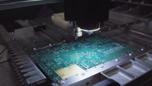
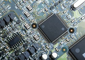
Surface mount technology (SMT) is an assembly process that places and solders electronic components onto the surface of printed circuit boards (PCBs). SMT assembly is highly automated using specialized equipment.
Component Sourcing
Electronic components must be procured from suppliers before they can be assembled onto a printed circuit board. When sourcing components, assemblers, and manufacturers consider factors like:
- Availability – Some components may be scarce or out of stock. Preferring more widely available parts can avoid delays.
- Lead times – How long it takes a supplier to fulfill an order. Parts with very long lead times can slow down production.
- Minimum order quantities – Suppliers often have minimum amounts that must be ordered. Buying excess parts increases inventory costs.
- Cost – Both the unit price and total spend are based on order volumes. Lower component costs increase profit margins.
- Quality – Using reputable authorized distributors reduces the risk of counterfeit or defective parts.
- Lifecycle status – Whether parts are actively manufactured or reaching end-of-life. Older components may need to be replaced eventually.
- Packaging – Components must be available in packaging compatible with production processes like automated SMT assembly.
Careful vetting and selection of suppliers is important to secure all the necessary components for assembly cost-effectively. Contract manufacturers often have established supply chain relationships to leverage for sourcing parts.
- SMT Assembly
- SMT Equipment and Process
The main pieces of equipment used in SMT assembly are:
- Solder paste printer – Applies a thin layer of solder paste on the PCB pads. The solder paste is a mixture of tiny solder balls suspended in flux.
- Pick-and-place machine – Uses small vacuum nozzles to pick surface mount components from reels and place them precisely on the solder paste-coated PCB pads. This machine places components extremely quickly and accurately.
- Reflow oven – Applies heat to melt the solder paste and form solder joints that attach the components to the PCB. The oven slowly ramps up to a peak temperature and then cools down using a controlled profile.
The SMT assembly process consists of:
- Solder paste is printed on the PCB pads.
- Components are picked from reels and placed onto the solder paste-coated pads.
- The PCB passes through the reflow oven, melting the solder paste to form solder joints.
Solder Paste Printing
During solder paste printing, a specially designed stencil is placed over the PCB and solder paste is applied to the stencil using a squeegee. The stencil has cutouts matching the pads on the PCB. This allows solder paste to be deposited on the pads when the stencil is removed. The thickness and quality of the solder paste print directly impact the reliability of the solder joints.
Pick and Place
The pick-and-place machine uses vacuum nozzles to pick components from reels and place them precisely onto their designated pads on the PCB. Components as small as 01005 chips can be accurately placed. The machine uses software files indicating the location and orientation of each component. High-speed pick-and-place machines can place over 135,000 components per hour.
Reflow Soldering
In reflow soldering, heat is applied to melt the solder paste deposits and attach the components to the PCB. Convection reflow ovens with multiple heating zones apply a precise thermal profile to the assembly. The profile gradually heats the assembly to the solder melting point and then cools it down. The solder joints solidify during cooling to form both mechanical and electrical connections. Factors like temperature and time impact solder joint quality. The oven atmosphere is also controlled to avoid oxidation.
Through-Hole Assembly
Through-hole assembly involves inserting components with wire leads into holes on the PCB and soldering them in place. This can be done manually or using automated equipment.
Manual Through-Hole Assembly
For low-volume PCBA, through-hole components can be inserted and soldered by hand. The operator will insert each component on the board, bending the leads slightly to hold them in place. The leads are then soldered to a pad on the opposite side to form an electrical and mechanical connection. This requires careful work to ensure the joints are properly formed. Any defects must be reworked by manually removing and replacing the component.
Automated Through-Hole Assembly
For higher volume production, automated equipment can be used for through-hole assembly. This includes machines for the sequential insertion of components, soldering using wave soldering or selective soldering methods, and cleaning flux residues after soldering.
Insertion machines have feeders for the components and use pick-and-place heads to automatically populate the PCBs. The boards then pass through an oven or wave soldering system to solder all joints simultaneously. For selective soldering, a focused solder wave or mini-wave is used to only solder specific joints. Cleaning systems remove any remaining flux using various methods.
Automated through-hole assembly ensures consistency and efficiency compared to manual methods. However, the equipment requires an upfront investment, and changeovers between PCB assemblies take time.
Testing and Inspection
Once the PCBA process is complete, rigorous testing and inspection is critical to ensure all quality standards have been met before the boards ship to customers.
Automated Optical Inspection (AOI)
Automated optical inspection, or AOI, uses high-resolution cameras and image processing software to visually inspect assembled PCBs and identify defects. The AOI system compares images of the assembled board to a “gold standard” image to check for missing, misaligned, or incorrect components. AOI provides rapid in-line inspection and can detect defects down to 0.025mm in size. This allows any issues to be corrected before further production.
In-Circuit Test (ICT)
In-circuit test, or ICT, uses probes to electrically test a completed PCB assembly against its electronic netlist. The ICT probes check each component for the correct value and that there are no short circuits or open connections. Any faults are identified before the board moves to functional testing. ICT provides electrical verification that components have been assembled correctly.
Functional Testing
Functional testing validates that the fully assembled PCB operates as intended. Boards are powered up and stimulated with inputs so their functions and performance can be verified against requirements. Issues like incorrect assembly or faulty components will result in functional failures at this stage. Functional testing provides the final quality check before shipping to ensure boards operate properly.
Thorough testing and inspection ensure all quality standards are met before delivery. Automated AOI, electrical ICT, and functional testing validate assembly integrity and reliability so customers receive boards that function correctly.
Read more: